A printed circuit board (PCB) is what replaces point-to-point wiring: an insulating board carrying copper tracks that connect components soldered permanently in place. Designing a PCB means turning a working schematic into a manufacturable physical board — reliable, compact and reproducible. This page is the way in to board design: it sets out the flow common to every tool (from schematic to manufacturing files) and points you to the design tool. Manufacturing itself (etching, drilling, plating) belongs to the workshop and to the course devoted to it. The wiki points at it without going into it.
What is it for?
A breadboard or a piece of perfboard is enough for prototyping, but they show their limits soon enough: intermittent contacts, bulk, a build nobody can reproduce, interference on fast signals. Moving to a PCB brings:
- reliability — soldered connections rather than wires that pull out;
- compactness — a dense build that fits in an enclosure;
- reproducibility — the same board, identical, as many times as you want;
- signal quality — controlled tracks, a ground plane, essential above a few kHz;
- production — the only realistic route to building several units.
A PCB is designed once the prototype has been proved on a breadboard and in simulation: the board freezes a solution that already works, it is not there for experimenting.
From schematic to board: the flow
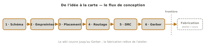
Whatever the tool, design follows the same sequence.
- Capture the schematic — place the components and their logical connections (schematic capture), as a clean schematic, then run the electrical rules check (ERC), which catches forgotten pins and inconsistencies before you go any further.
- Assign the footprints — every component on the schematic has a physical footprint (the shape of the pads and the real pitch of the package). A wrong footprint means a component that will not fit.
- Place the components on the surface of the board — group them by function, think about ergonomics (connectors at the board edge, heat dissipation).
- Route the tracks — draw the copper that carries out the schematic’s connections, by hand or with the help of an autorouter.
- Run the design rules check (DRC) — track width, minimum clearance, pads: an automatic check catches mistakes before manufacturing.
- Generate the manufacturing files — the Gerbers (copper layers, silkscreen, solder mask) and the drill file, which describe the board to the manufacturer.
- Manufacture — etching and drilling in the workshop, or an order placed with a manufacturer. This stage is outside the scope of the wiki (see the manufacturing course and workshop).
Single, double or multilayer
The number of copper layers depends on the density and on the signals.
- Single-sided (1 layer) — the easiest to manufacture, enough for a build that is not dense; routing sometimes acrobatic (wire links).
- Double-sided (2 layers) — the standard for a student project: two routing planes, room for a ground plane, a good compromise.
- Multilayer (4 layers and more) — for high density and fast signals (internal ground and supply layers); rarely needed at the scale of a school project.
Choosing a tool
An EDA package (Electronic Design Automation) covers the whole flow, from schematic capture to Gerber export.
| Tool | What sets it apart | When to use it |
|---|---|---|
| KiCad | free, open source, complete, cross-platform, the standard | serious board design, for the project and beyond |
| EasyEDA | the footprint comes with the component, offline mode | the school’s tool, right through to etching in the lab |
For a project going out to an external manufacturer, KiCad is the default choice: free, unlimited, and widely documented. For a board etched at school, EasyEDA is what is used, and its page goes as far as the file handed to the workshop.
Note
Designing is not manufacturing. The wiki covers design, from the schematic through to the files handed to whoever does the etching. The physical manufacture of the board (etching the copper, drilling, plating the holes, silkscreen) belongs to the workshop and to the manufacturing course. The boundary is the manufacturing file: what the designer produces, what the manufacturer consumes. Its format depends on who is doing the manufacturing. With an external manufacturer, it is the Gerbers. At school, the workshop works from an EasyEDA
.jsontogether with the schematic (see EasyEDA).
Pitfalls
Routing before the schematic is frozen. Any change to the schematic after routing means redoing the tracks. You only route a schematic that has passed the ERC.
A wrong footprint. Assigning the wrong footprint (wrong package, wrong pitch) gives you a board the real component will not solder onto. Check every footprint against the component’s datasheet.
Forgetting the ground plane. A ground routed as a thin track, awkwardly shared, generates noise and floating references. A ground plane (a dedicated copper area) steadies the signals.
Undersizing a power track. A track too thin for the current it carries heats up, and can melt. Supply and power tracks are wider (see the track-width charts).
Ordering without reviewing the output. A Gerber viewer shows the board as it will be etched. One last look saves you from committing a whole batch of wrong boards. At school, the same check is done by printing the board at 1:1 scale and laying the components on it.
Where it fits in the project
- Proof of concept phase — the build is proved first on a breadboard and in simulation, and the PCB comes afterwards, to freeze the solution chosen.
- Technical design file phase — board design (RA-PROJET-C03-3/EEE/5) belongs here: this is where you design and build the board that brings together microcontroller, sensors and actuators (see energy and information chains).
- Manufacturing interface — the manufacturing file is the deliverable handed to the workshop or to the manufacturer, the boundary with the manufacturing course. Gerbers with an external manufacturer,
.jsonand schematic at the school workshop.
See also
- KiCad — the open-source tool for designing a board (tool tutorial)
- EasyEDA — the school’s tool, from schematic through to the board etched in the lab (tool tutorial)
- Analysing a circuit schematic — the schematic you capture before routing (prerequisite)
- Circuit simulation — proving the build before drawing the board
- Reading a datasheet — where footprints and component constraints come from
- Microcontroller — often the heart of the board being designed
- Energy and information chains — what the board carries out physically
- Technical design file — where the board design is recorded