EasyEDA is a printed circuit board design tool. You draw the schematic of a circuit, then you turn that schematic into a real copper board, ready to be manufactured. Everything happens in the same window, from the first stroke to the file you hand over to the workshop.
This is the tool we use at school, and this page goes all the way. It takes you to the board milled on the lab machine, the one you will take away to solder. The constraints described here are therefore its constraints, not those of an outside manufacturer. The printed circuit board hub carries the general flow and the vocabulary. Here you learn the gestures, in the order you perform them. Keep the software open beside you.
Note
The interface speaks two languages. The main menus are in French, such as Fichiers, Placer or Réglages, that is File, Place and Settings. But many entries have stayed in English, sometimes inside the same drop-down, such as Design, Check DRC, Copper Area or Run Mode Setting. Do not look for a logic, there is none. The paths are written here exactly as they appear on screen, mixture included.
What is it for?
A board is not drawn in one go. You proceed in stages, and EasyEDA holds them all.
- Draw the schematic, and make it readable. You name the connections instead of dragging wires from one end of the sheet to the other.
- Give each component a footprint, that is the space it will really occupy on the copper. When it does not exist, you draw it yourself.
- Place and route, under the rules of the machine that will mill the board.
- Have the routing checked by the software, before any copper is cut.
- Export the file the workshop will consume.
What makes it special fits in one sentence. The component you place arrives with its footprint. On KiCad, you first pick a symbol, then you go and fetch a footprint for it in another library. If you get it wrong, you find out once the board is milled, when the part does not fit its holes. Here the symbol and the footprint travel together, and a whole family of mistakes disappears at once.
Do not take that for a gift. You become dependent on what the catalogues contain. The day your component is not in them, you will have more work than elsewhere. We will see how to get out of it.
A word about what this page will not do. EasyEDA ships with a simulator, and we will not touch it. To try a circuit out before routing it, Falstad and LTspice do that far better, and the circuit simulation hub takes you there.
Installing, and switching to offline mode
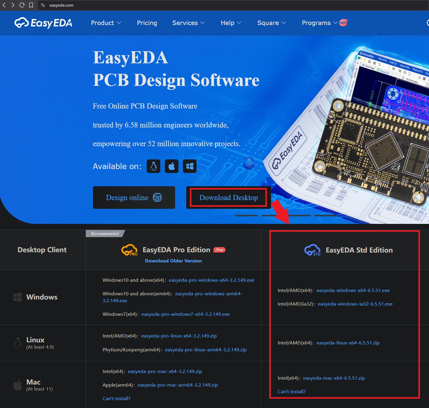
Go to the EasyEDA website and click Download Desktop. You land on a two-column table, one per edition, with the download links for each system. Take the right-hand column, EasyEDA Std Edition, and the link that matches your machine.
Warning
The site pushes you towards the wrong edition. The left-hand column, Pro Edition, carries a
Recommendedlabel. That is the site’s recommendation, not ours. The two editions share neither the same interface nor the same menus, and their files are not interchangeable. This whole tutorial is written for the Std Edition, the one in the column outlined in red on the picture. If you install the Pro, nothing that follows will look like your screen.
On first launch, a Run Mode Setting window asks which mode you want to work in. Choose Project Offline Mode, then Apply. The software then asks for a restart. Accept.
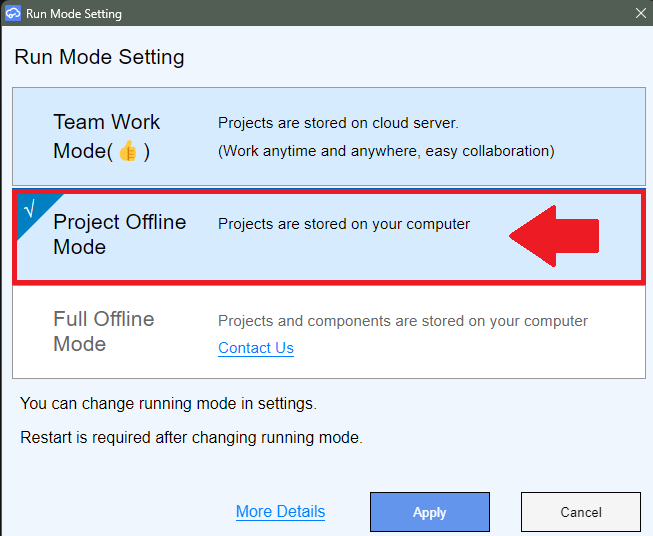
That is all there is to do here, and it is the one thing not to miss. Once the choice is made, the words Projects Offline mode appear at the top left, next to the name of the software. If they are there, you are ready.
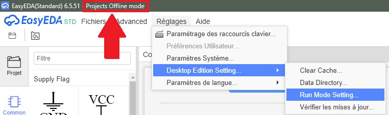
If they are not, the same window reopens through Réglages → Desktop Edition Setting… → Run Mode Setting…, that is Settings → Desktop Edition Setting, as above.
Building the board
You are going to make a complete PCB, from the blank sheet in the software to the finished board you will solder yourself. Today the tutorial shows you how, using a circuit called an NE555 astable. It is a circuit that makes an LED blink, with six components, all through-hole. It was chosen because it routes without difficulty, and because at the end, board in hand and iron beside you, you will see the LED blink for real. Understanding the theory of the astable is not needed to follow along. Here the subject is the board.
1. The project, the sheet and the title block
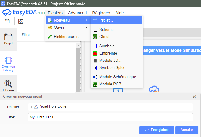
Fichiers → Nouveau → Projet…, that is File → New → Project. Take a look at that same submenu on the way. It also offers Schéma, Circuit and Empreinte, that is Schematic, Board and Footprint. Remember where they are, we will come back for the last one.
Give your project a title and leave the folder on Projet Hors Ligne, that is the offline project folder.
Your project contains one sheet, Sheet_1. That is where the schematic is drawn, and it looks a lot like what you saw in your electronics classes. A red frame marks out the working area, bordered with reference marks. Numbers along the top and bottom, letters down the sides. They are there so you can point at a place in the schematic out loud, something like “look at B3”. In the bottom right corner sits the title block.
Fill it in straight away. It is one minute of work and it will follow you through the whole project. The project name, your group number, the date, your name.
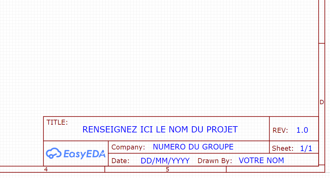
There is nothing administrative about it. In a design office, the title block is what makes a document traceable. Without it, nobody knows, three weeks later, which version of the schematic they are looking at or who to ask about it. The revision index (REV) is there for that. You will move it to 1.1, then to 1.2, as the schematic evolves. It is the same requirement as on any item filed in a technical design file.
Tip
Keep the placement conventions from your electronics classes. Inputs on the left of the sheet, outputs on the right, positive supplies at the top, grounds at the bottom, and the useful components in the middle. This is not a question of looks. A schematic that respects these conventions reads effortlessly to somebody who did not draw it. Your project partner, your supervisor, or yourself after the holidays. See Reading a schematic.
2. Searching for a component, and reading what you find
Placer → Symbole, that is Place → Symbol, or faster still Shift+F, opens the search window. Type the name of the component. It takes at least three characters for the search to start.
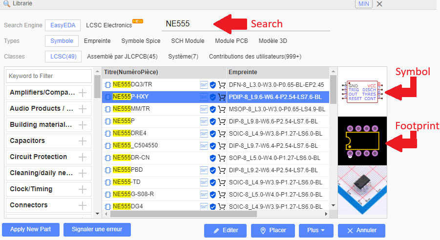
The Types row decides what you are looking for, a Symbole, an Empreinte or a 3D model, that is a symbol, a footprint or a 3D model. Stay on Symbole. That is the one that goes onto the schematic, and the footprint comes with it.
Just below, the results are sorted into classes, each with its number of hits. They are not equal:
- LCSC and Assemblé par JLCPCB are maintained by professionals. What you find there is reliable and complete;
- Système holds the generic components shipped with the software;
- Contributions des utilisateurs, the user contributions, is filled by other users. It is by far the largest. On
NE555it shows 999+ where the other three together give one hundred and one. It is also an attic. There is very good work in there, and sloppy work, and complete parts, and unfinished ones, all mixed together.
You will often end up searching in it anyway, for lack of finding anything elsewhere. Hence the reflex, to pick up right now and to keep: look at the right-hand panel and check that the part really has a symbol and a footprint. The symbol shows at the top, the footprint below.
Warning
A component without a footprint does not show up on the schematic. It places normally, it wires normally, everything looks fine. The fault only appears when you move to the board, when one footprint is missing where all the others have one. The glance at the right-hand panel costs you two seconds. Finding out later will cost you a full rework.
Tip
For passive components, use the tree on the left. It sorts resistors, capacitors, connectors and the rest by family and by technology. It is quicker than guessing a part number, and it shows you along the way everything that exists under a single word.
3. The footprint, and why the part number matters less than it does
This is where the success of your board is decided, and it rests on a distinction that many people grasp too late.
The symbol is what you place on the schematic: a rectangle, a triangle, a zigzag, with named pins. It says what the component does. The footprint is what will appear on the copper: pads, at such and such a distance from one another, drilled or not. It says how much room the component takes and how it is soldered.
All three sit well side by side on the NE555:
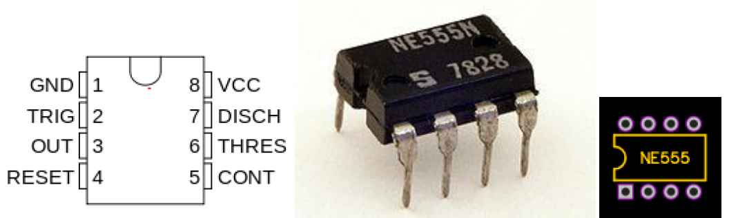
The symbol tells you what each pin is for. The photograph shows the object you will hold. The footprint knows nothing but holes and distances. It has no idea that this is an NE555.
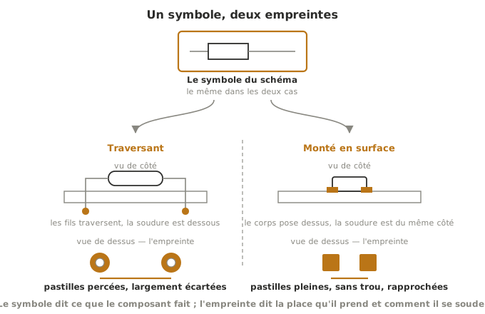
The consequence is surprising at first. The exact part number matters far less than the footprint. You will not find your 10 µF capacitor in the catalogue with the right dielectric, the right voltage and the right brand. That does not matter. What you need is a footprint that matches the component you have in your hand. Two holes at the right spacing, and you will solder the real capacitor into them. The value written on the schematic drives nothing on the copper.
Tip
Push the reasoning to the end. A footprint belongs to nobody. A through-hole resistor and a through-hole capacitor are both “two holes”. If you cannot find a satisfactory footprint for one, take the other one’s. All that matters is that the spacing matches what you are going to solder. The copper does not know what will come and sit on it, and it does not care.
One precaution only, and it comes at the soldering iron. The silkscreen on the board will read
R4at the place where you must solder a capacitor. Write it down somewhere, or you will fool yourself three weeks later.
Warning
A wrong footprint cannot be recovered. A wrong value, you fix at the iron by changing the component. A wrong pad spacing gives you a board where the part does not fit, and there is nothing to be done. It is the only mistake on this page that costs a copper blank. Check against the dimensions in the datasheet, or failing that with a caliper on the sample you have to hand.
For every component, one single question to ask yourself: what I am going to solder, does it fit in there?
And that question is less obvious than it sounds, because the same word covers very different objects. “A capacitor”, for instance:
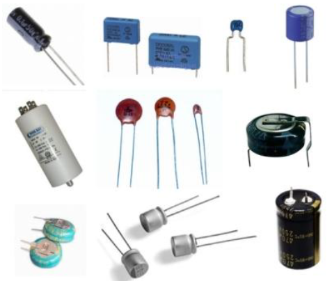
Electrolytic, ceramic, film, tantalum. What size, what lead spacing, what voltage? At this stage you probably have no idea, and that is fine. Take the one you have in your hand, measure the spacing of its leads, and look for a footprint that matches it.
What that changes shows up at the soldering iron:
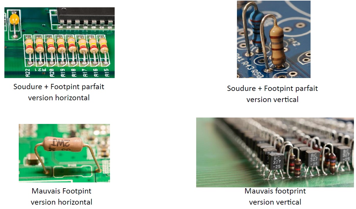
A correct footprint gives a component that sits down and solders effortlessly. A wrong footprint gives twisted leads, forced apart, sometimes broken. And a board you would rather not show anybody.
4. Through-hole, and nothing else
Here is the most important rule on this page, and the one that does the most damage when it is forgotten.
Your components must be through-hole. Not surface mount, not SMT, not SMD. This is not a matter of style. We do not have the equipment to solder SMD at school. An SMD component picked by mistake gives you a board you will not be able to assemble, and you will only find out once the copper is milled, the board in your hand and the iron switched on.
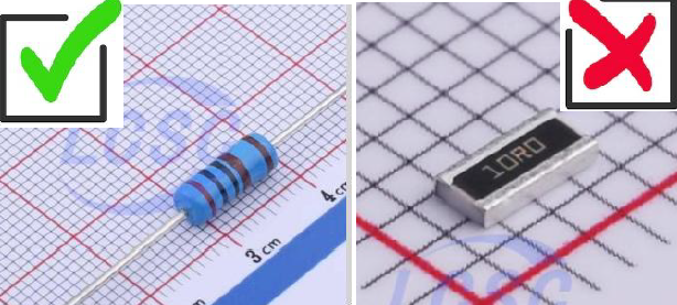
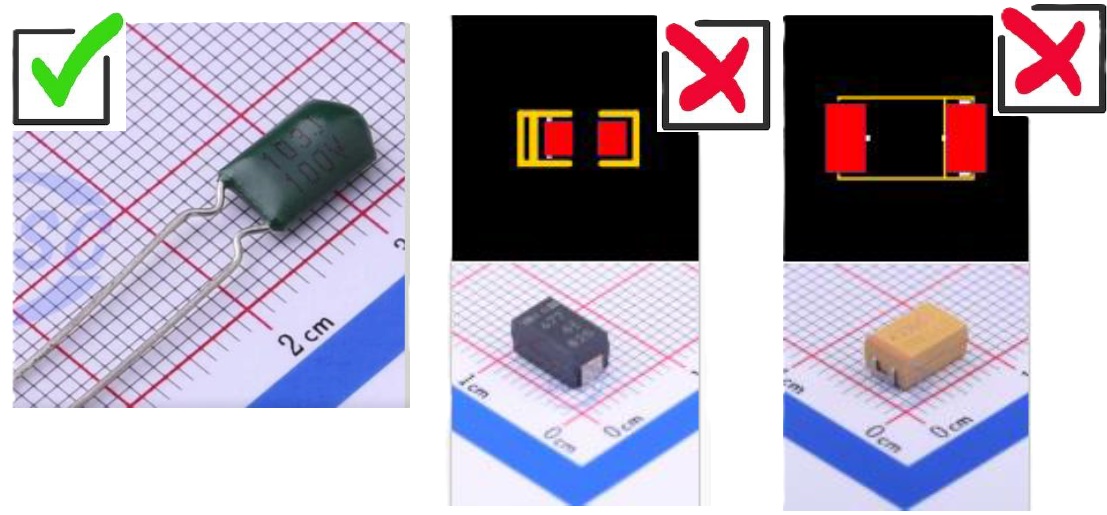
Three ways to check, from the most reliable to the quickest:
- Look at the footprint preview, in the right-hand panel. Drilled pads mean through-hole. Solid pads, with no hole, mean SMD. It is the most reliable criterion, because it shows you the thing itself.
- Read the name of the footprint, in the middle column.
RES-TH_,CAP-TH_,DIP-8,PDIP-8. TheTHstands for through hole, and aDIPpackage is through-hole by construction. ConverselySOIC-8,SOP-8,MSOP-8,DFN-8, or a four-digit code such as0603,0805,1206, mean SMD. - Use the tree on the left, which already sorts the families by technology.
Warning
Do not trust the
SMTtag in the list. It also appears on perfectly through-hole parts. It refers to an assembly service, not to the technology of the component. The hole in the pad, on the other hand, does not lie.
For every part you select, the reflex is therefore double, and it takes two seconds: is there a footprint? does it have holes?
5. Wiring the schematic
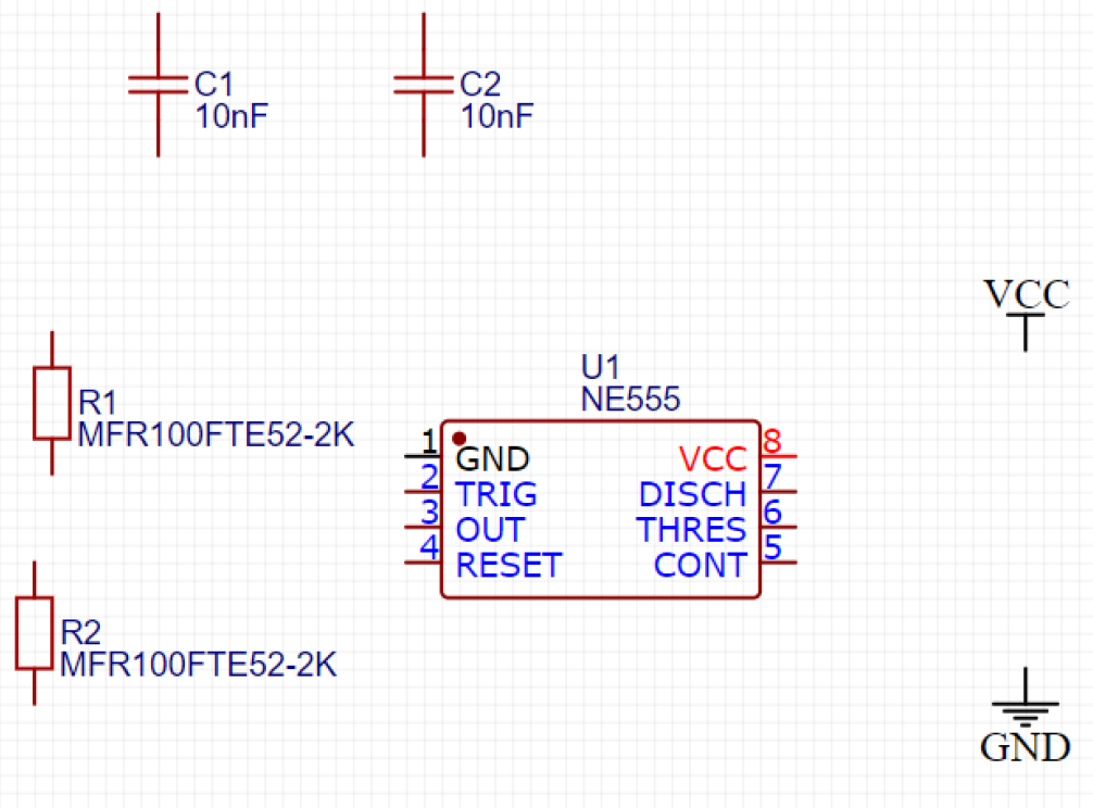
Place your components on the sheet: the two resistors, the two capacitors, the NE555. Do not look for the perfect layout yet, you will move them around.
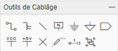
You also need the supplies. They are not drawn like components. The Outils de Cablâge toolbar, that is the wiring tools, at the top right of the sheet, offers dedicated symbols to be placed like the rest: VCC, +5V, ground.
Warning
These supply symbols are not decoration. They are how the software understands that a wire is a ground or a supply. If you simply drag wires between pins without ever placing a
VCCor aGND, everything will look right on screen. It will jam further on, when you move to the board, and you will have to redo the wiring from the start.
That leaves connecting it all up. The Wire tool draws the wires from one pin to another. Where two wires genuinely meet, a red dot appears. It is the only mark that tells a crossing from a connection, so look at it.
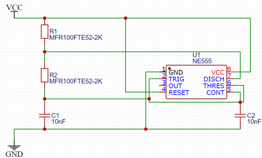
It is correct, and it is unreadable. Now imagine the same job with a forty-pin microcontroller. The schematic turns into a plate of spaghetti where nobody can find anything.
A mistake has crept into this wiring. Can you find it?
Look at the wire carrying
TRIGandTHRES, pins 2 and 6, down to capacitor C2. There is a red dot where they cross, so a connection. And that connection takesTRIGandTHRESonto pin 5,CONT.That link does not exist in the reference circuit. The two wires must cross without touching. One red dot too many, and the circuit no longer does what it is asked to do.
That is the whole problem with wiring by hand. The junction point is tiny, it appears with a single misplaced click, and nothing flags it. The software takes your word for it.
6. Naming connections instead of dragging wires
The remedy is called the net label, the Net tool. The principle is simple and it changes everything. Two wires carrying the same name are connected, even if they do not touch on screen.
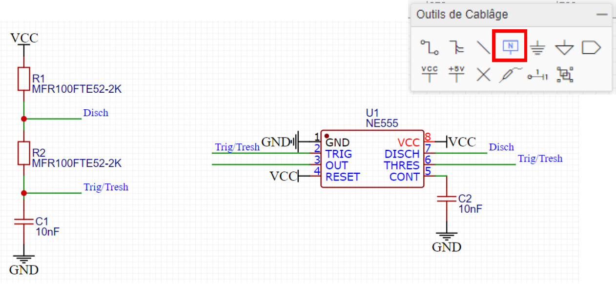
Compare the two pictures. It is the same circuit. The second one reads at a glance, because it is cut into pieces you can understand separately. The R1, R2, C1 chain on one side, the component on the other.
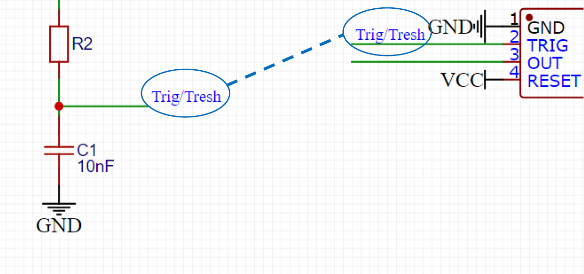
And the name you choose does half the work. Look at Disch or Trig/Tresh. Each label says what the wire is for, not where it goes. A reader who sees Trig/Tresh on pin 6 knows immediately that it joins the midpoint of the RC network, without having to follow anything with a finger.
Tip
A named connection is added without redrawing anything. Need to hook something else onto the supply? Place a
VCClabel on it, and it is connected. That is what makes a schematic modifiable, and you will modify it, several times.
7. An output you can see
As things stand, the OUT pin of the NE555 goes nowhere. The circuit oscillates, and nothing shows it. So let us add an LED, which will make the blinking visible. It comes with its series protection resistor, without which it would not survive long.
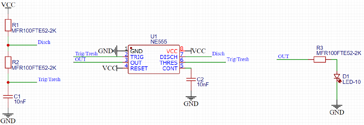
Look at how the output got connected: an OUT label on pin 3, an OUT label in front of R3, and it is done. No wire crossed the sheet, and the new block reads on its own.
Note
Changing a value on the schematic changes nothing on the copper. You can write whatever you like on R1 or C1, the milled board will be the same. Only the footprints count. The real circuit will depend only on the components you solder onto it. So you will be able to adjust the blink rate at the iron, without touching the board.
8. Getting the current in
There is one question that is easy to forget: where does the current come from? The VCC and GND symbols tell the software what a supply is, but they do not make electricity. You need a physical place where the cable arrives.
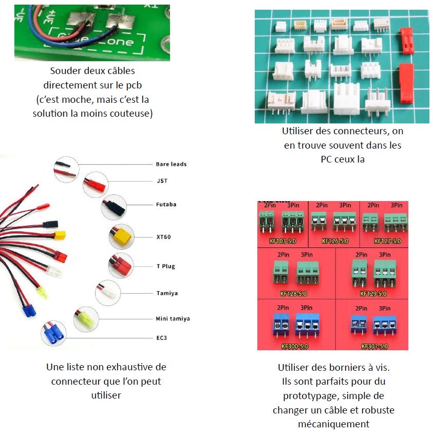
Look for a two-pin connector. A screw terminal does the job perfectly for prototyping.
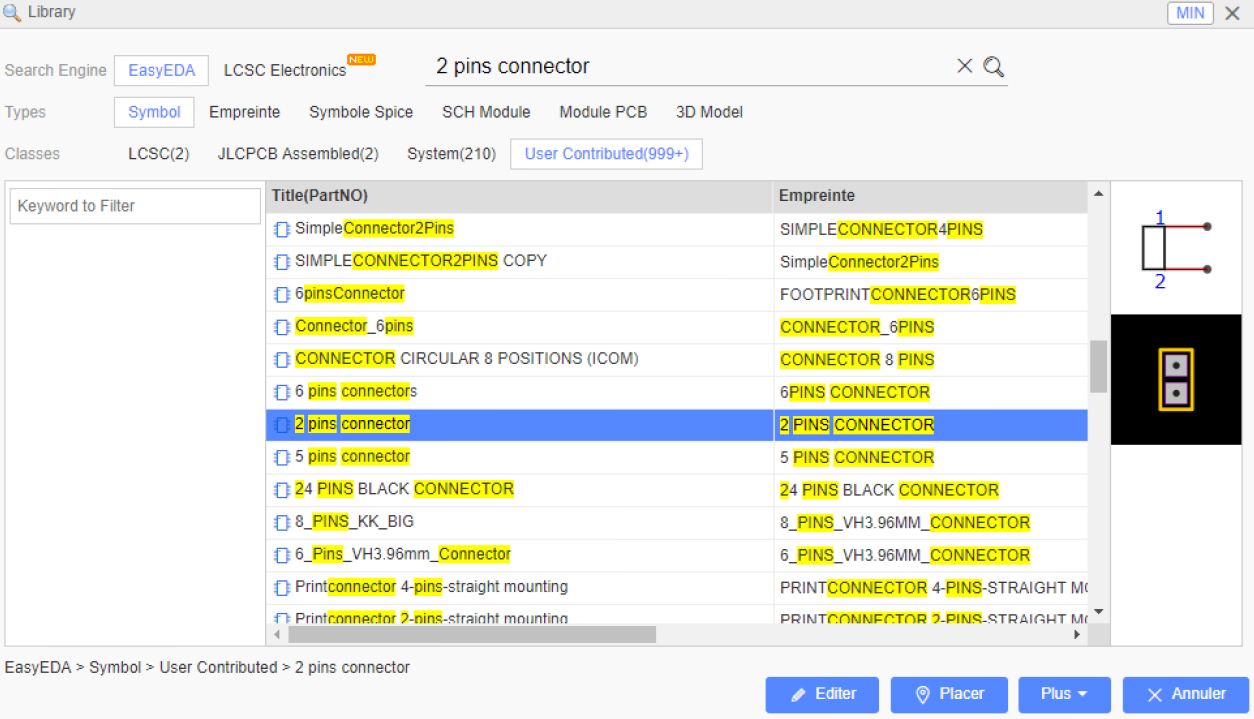
Take the opportunity to observe the quality of the results. The search returns connectors with five, six, eight and twenty-four pins for a two-pin request. That is the attic we were talking about. Sorting is up to you, and the footprint preview is your best tool for it.
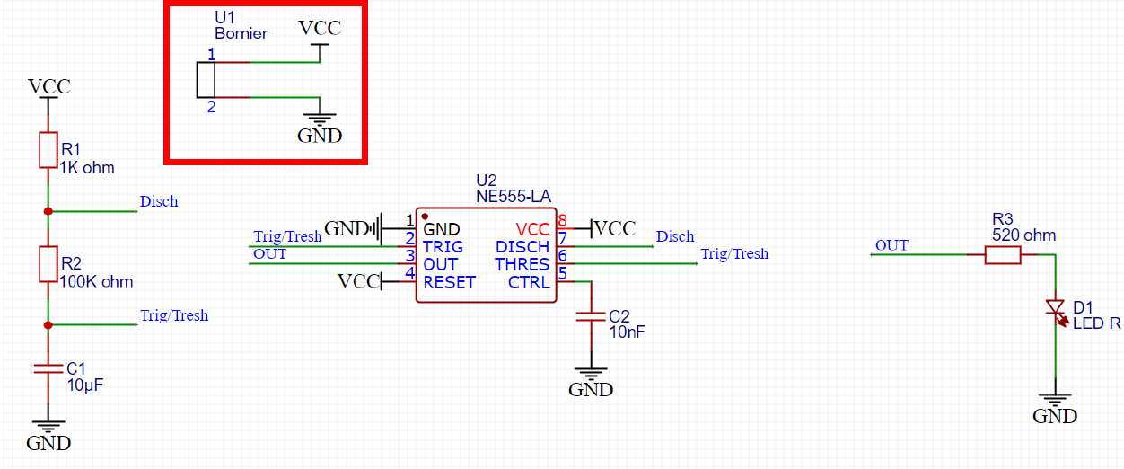
And there is the whole point of labels: adding the terminal required no change anywhere else on the schematic. Two supply symbols on its pins, and it is connected to everything carrying VCC or GND.
That terminal is only an entry point. What you plug into it stays open.
Tip
The screw terminal is the right choice for prototyping. It holds mechanically, and above all it comes apart again. Changing a cable needs neither a soldering iron nor desoldering braid. Soldering the wires straight onto the board works too and needs no extra part, but what you have soldered, you will have to desolder.
9. Moving from schematic to board
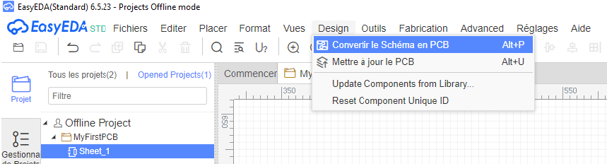
The schematic is finished. Design → Convertir le Schéma en PCB, that is Design → Convert Schematic to PCB.
Danger
Never take
Mettre à jour le PCB, that is Update PCB. It is the line just below, it describes better than the other one what you will want to do, and it is a trap. In offline mode, the update does not exist. The software runs a check, then asks you to log in and go back online. If you accept, you lose access to the community libraries. And you will not connect that click with the consequence until much later.To carry a schematic change over to the board there is only one path: run
Convertir le Schéma en PCBagain, which starts from a blank page.
Hence a consequence to be taken seriously. Your schematic must be right before you convert. Everything you do on the board afterwards will be lost if you have to convert again, whether it is the placement, the routing or the ground plane. Read it through one last time now.
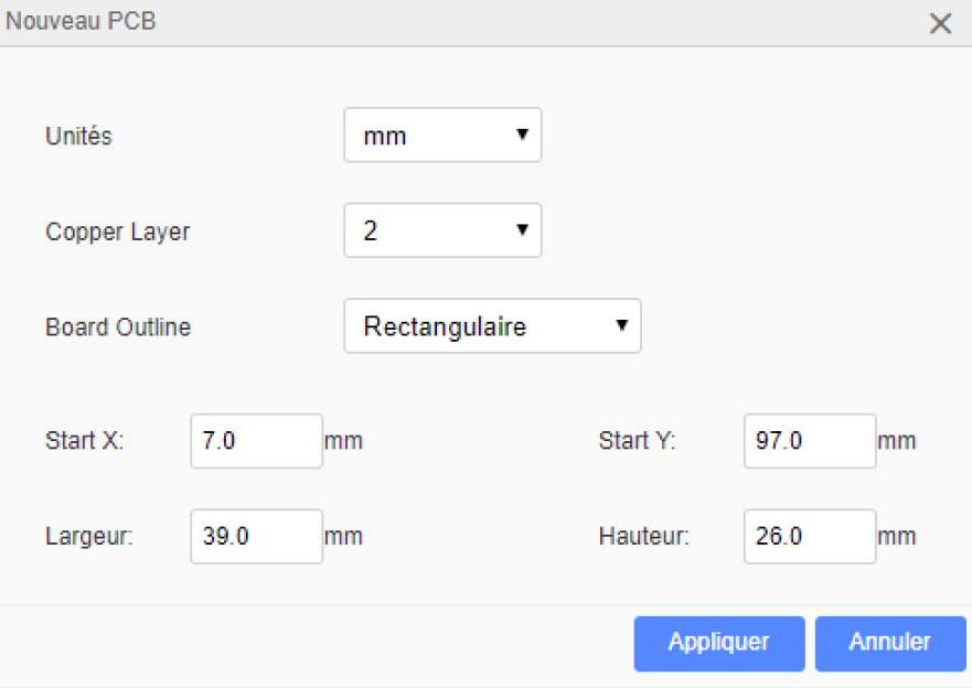
A window asks you for the characteristics of the board. You have nothing to change in it.
10. The ratsnest, and the placement
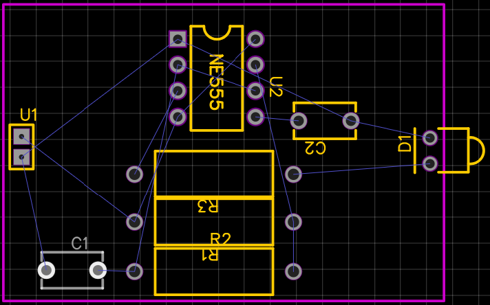
A new file opens, and it looks like nothing you know. A purple frame marks out the surface of your future board. Below it, the footprints of your components, in a heap. And between them, a web of thin lines going in every direction.
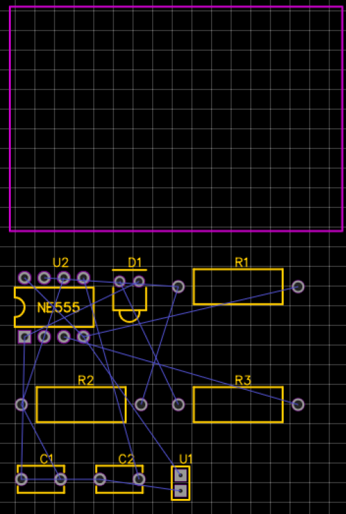
Those lines are called the ratsnest. They are not tracks. They are the connections your schematic declared, and that you will have to draw in copper. The ratsnest is your shopping list. Every blue line you make disappear is one connection done.
Start by bringing the components inside the purple frame. Nothing forces you to place them cleverly yet. The only constraint for now is that they must not overlap.
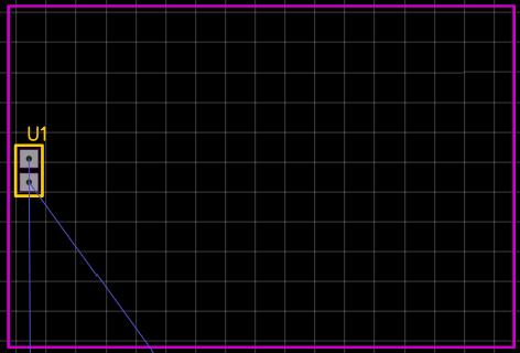
Place terminal U1 first. It brings the current in, so give it an edge of the board. The cable has to arrive from outside.
Then bring in the rest.
Tip
Keep the same logic as on the schematic: what comes in on one side, what goes out on the other. The supply terminal against one edge, the LED against the opposite edge. A board whose direction you can guess just by looking at it is a board you wire without making mistakes.
11. The rules of the machine
Before drawing a single track, you have to tell the software what the milling machine can do. Design → règle de dessin, that is Design → design rule.
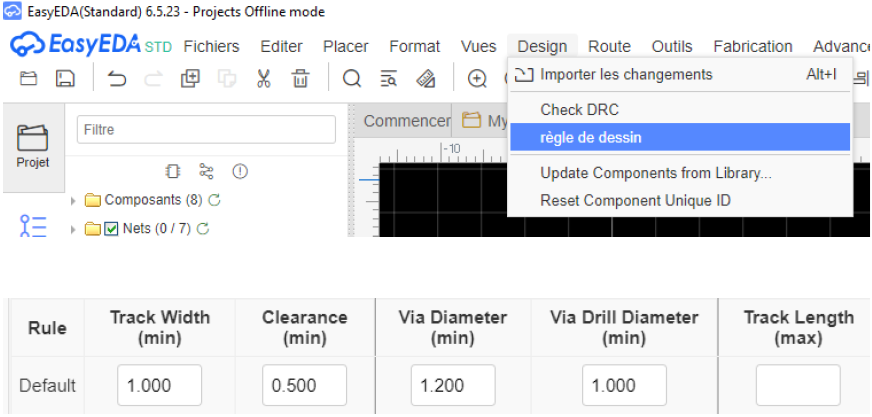
These numbers are not preferences. Each one describes a physical limit of the tool that will mill your board:
| Rule | Value | What it means |
|---|---|---|
Track Width (min) | 1 mm | The thinnest track the cutter can draw |
Clearance (min) | 0.5 mm | The minimum gap between two coppers that must not touch |
Via Diameter (min) | 1.2 mm | The minimum diameter of a through-hole pad |
Via Drill Diameter (min) | 1 mm | The diameter of the drill bit fitted to the machine |
Note
These values are far wider than in industry. A professional manufacturer goes ten times lower. That is not a handicap, it is a design constraint like any other. Designing under a known constraint is better than designing under no constraint at all. You will find that at 1 mm of track, room runs out quickly, and that is where placement becomes interesting.
12. Pads you can actually solder
One last preparation before routing, and it comes from experience at the soldering iron: the larger the copper area, the easier the solder joint. The default pads are small and round.
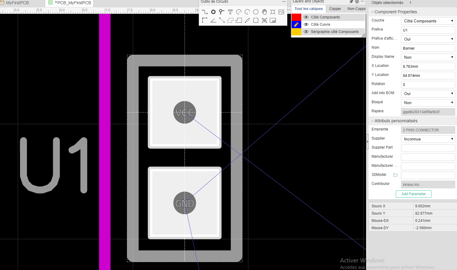
Click on a pad, and its properties panel opens on the right. Set it to a 3 mm by 1.5 mm rectangle, and set its drill to 1 mm. The rectangle is a setting proven by previous cohorts: wide enough for a soldering iron to heat the pad without trouble, narrow enough not to eat the room needed by neighbouring tracks. The millimetre, for its part, is the diameter of the drill bit fitted to the machine.
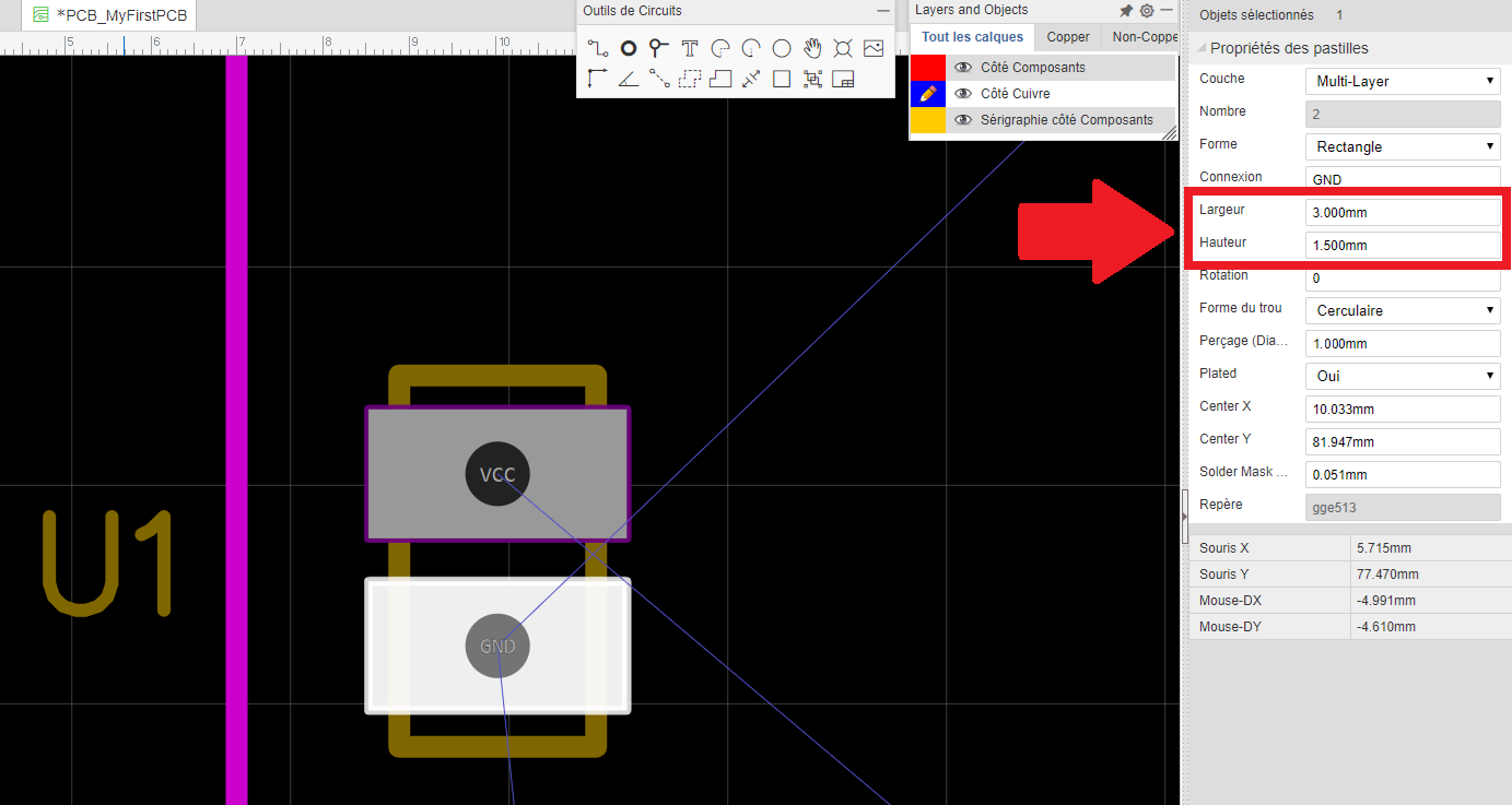
To be done on every pad on the board. Your board then looks like this. Same components, same provisional placement, but pads a soldering iron can get a grip on.
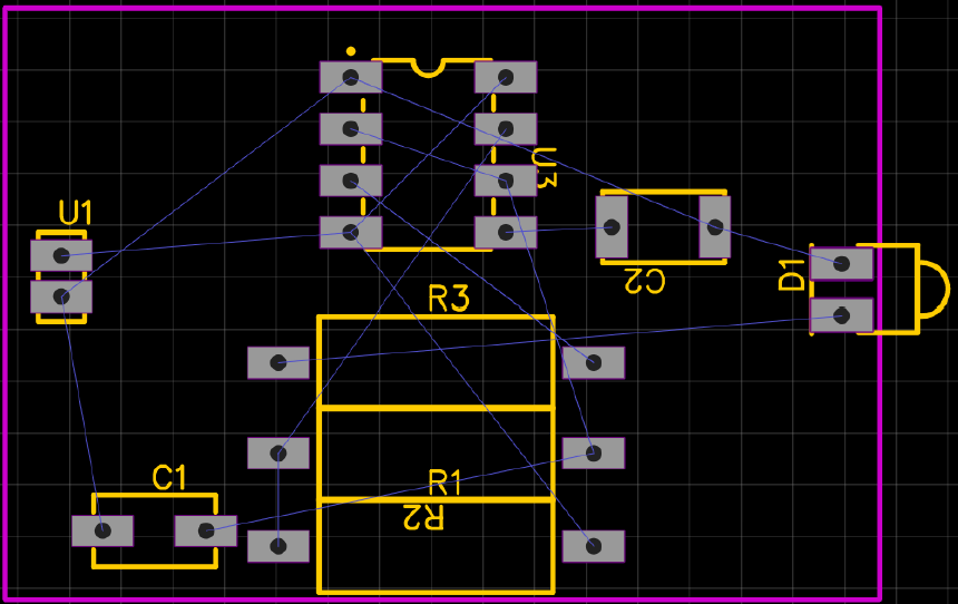
Warning
Draw the holes at the size they will really be. The workshop machining routine imposes its own diameters, whatever your file contains. That will be 1 mm for the pads and 3 mm for the mounting holes. So what you type does not drive the machine.
But it does drive what the software shows you and what it checks. A hole drawn smaller than it will be drilled hides a very real collision from you. On screen the track passes beside it, and on the board the drill cuts it. You will only find out once the copper has been cut.
Simple rule: the drawing must tell the truth about the geometry, even when somebody else is holding the cutter.
Tip
The rectangle has a direction. Depending on how the component is oriented, you may have to swap width and height. Count 3 mm in the direction the track arrives from, 1.5 mm in the other. A pad stretched at right angles to its track is of no use.
13. Routing the first track
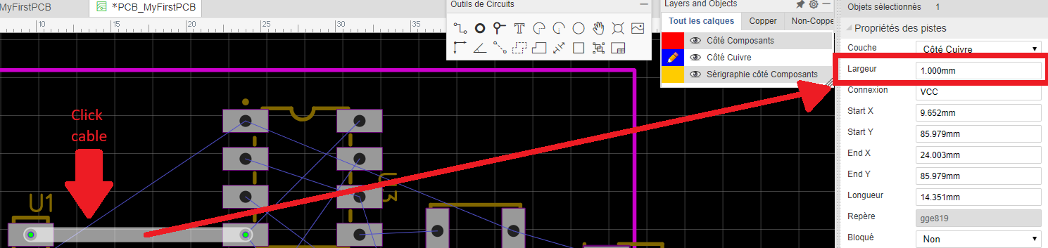
Here we are. The Wire tool, shortcut W, draws the copper from one pad to another. One single thing to check before you start: that you are indeed drawing on the Côté Cuivre layer, that is the copper side, the one that will be milled.
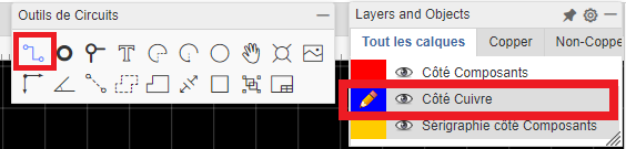
Before you launch in, a reflex that will save you hours. Move the components so that the ratsnest line is straight. Two pads to be joined that are not aligned will force you into detours. Aligned, the track draws in one stroke.
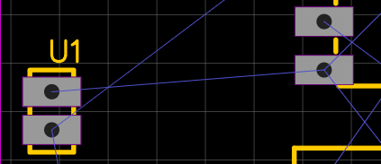
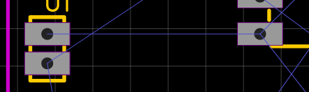
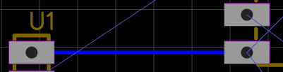
Now draw the connection. The blue ratsnest line disappears and a copper track appears in its place.
Check its width: click on the track, and read the right-hand panel. It must be 1 mm, the minimum value the cutter can draw.
Then start again, ratsnest line after ratsnest line. The R key rotates a component, and the ratsnest reorganises itself as you move the parts around. It is often better to move a component than to go around an obstacle.
Tip
Leave
GNDfor the end. It is the net that touches almost every component, and therefore the one that will get in the way most if you route it too early. We will deal with it differently, right at the end.
14. Two 45° turns are better than one right angle
Sooner or later, a track will have to turn. When that happens, turn it in two steps of 45° rather than one of 90°.
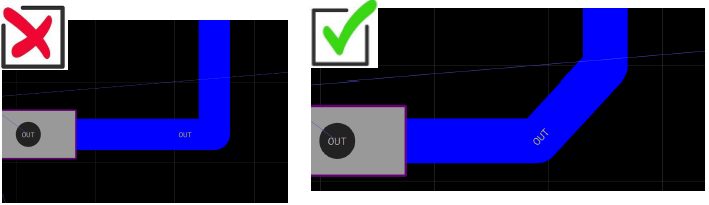
Let us be honest straight away. On your board, the right angle will cause no problem at all. An LED blinks far too slowly for the shape of the corners to have the slightest effect. So why ask you for 45° anyway? There are two reasons.
The first one is historical. Boards used to be etched in acid. A little product stayed trapped in the inner corners and went on eating away the copper after the bath. It was called an acid trap. Your board is milled and not etched, so that problem does not concern you.
The second reason is the good one. It is a professional reflex, and a reflex is acquired where it costs nothing. One day you will route a board that communicates, over Wi-Fi, over radio or with a fast bus. That day, the shape of your tracks will stop being a cosmetic detail. You will be glad to have the gesture already in your fingers.
Note
A track becomes an antenna through its length, not through its bends. Look at the Wi-Fi antenna of an ESP module. It is a copper track folded like an accordion. The folds only serve to fit a length tuned to the transmitted frequency into a small space. What radiates is that length. A short, angular track does not radiate. A long, perfectly straight one does.
15. Getting through where there is no room
Your board has only one copper face. Two tracks therefore cannot cross, they would touch. Routing quickly becomes a puzzle, and two tricks unlock it.
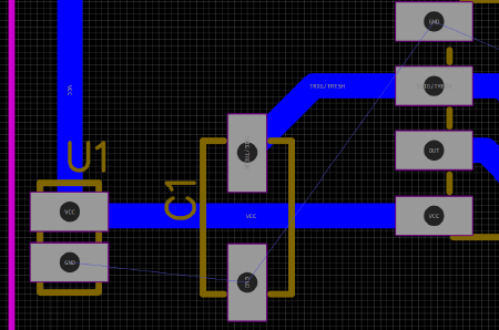
The first one: pass underneath a component. A board is a three-dimensional assembly. Between the legs of a package there is empty space, and a track can go through it without touching anything.
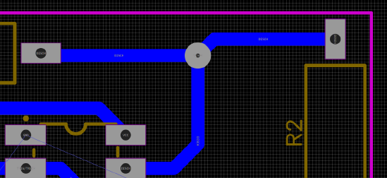
The second one: add an intermediate pad when several tracks have to meet. Rather than piling up bends around a meeting point, you place a pad and everything converges on it cleanly.
16. The jumper wire, when you really have to go over the top
When no detour works, there is still the jumper wire: a wire that you will solder over the board, between two pads, to get across an existing track. The connection no longer goes through the copper, it goes through the air.
In the software, you draw it by cheating. You draw that piece of the connection on the component side, where there is no copper, and two pads act as anchors at each end. On screen, that segment appears in another colour.
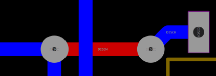
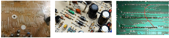
That red will not exist on the milled board. It is up to you to solder a piece of wire between the two pads, once the board is in your hands. Nothing tricky about it, and the technique is as old as consumer electronics.
Tip
Aim for fewer than ten jumper wires. This is not a physical threshold, it is a placement quality target. Every jumper is a wire soldered by hand, so extra assembly time and one more point of mechanical fragility. Beyond about ten, it is a sign that your components are badly laid out. It is often quicker to move two of them than to solder eight wires.
17. The mounting holes and the machine origin
Two finishing details, both of them essential.
First, the mounting holes: the ones that will take the screws holding the board in an enclosure or on a mechanical assembly. Put one in each corner, and set their drill to 3 mm, the diameter the machine will give them.
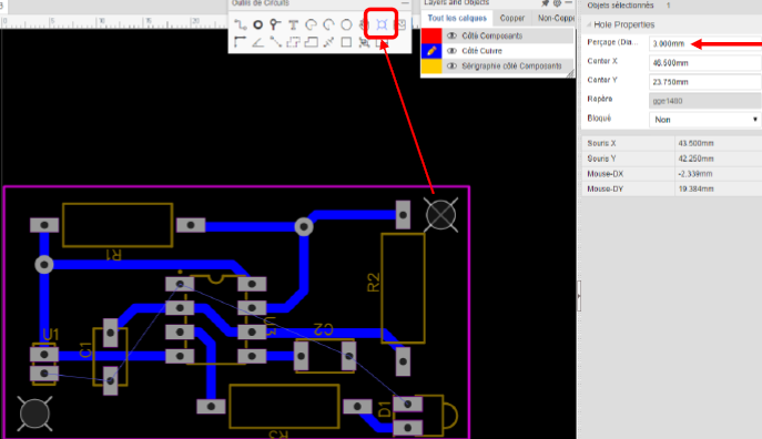
This is where the warning in section 12 takes on its full meaning: a hole drawn smaller than it will be drilled would suggest the neighbouring track gets through, when in fact the drill would cut it.
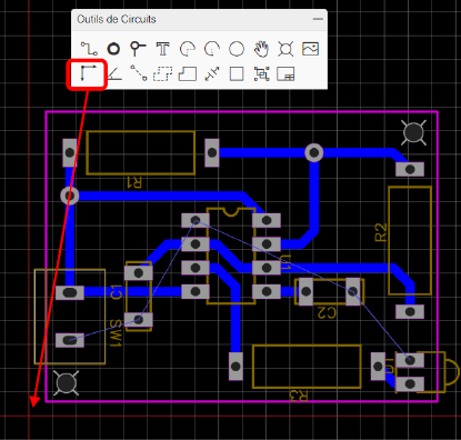
Next, the origin of the working area. The milling machine needs a reference point to know where to start. Put it at the bottom left of the board.
18. The ground plane
You have been leaving GND aside from the start. Here it is. Looking at the board, some ratsnest lines are still undrawn. Those are the ones.
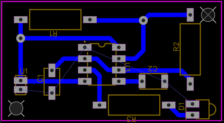
We are not going to route them one by one. Instead, we fill all the remaining copper with ground: that is the ground plane. The Copper Area tool, shortcut E, asks you to click the four corners of the board, then Échap to close, that is Escape. A box then asks which net to attach the area to: GND.
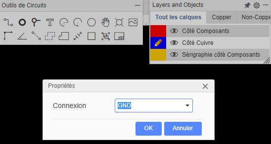
All the free space becomes copper connected to ground, and the GND connections make themselves.
Warning
Check that only one is left. Depending on your placement and the clearance set in the design rules, the fill can end up cut into several islands that nothing connects. Each one is a separate ground plane, and the connections between them are not made. The ratsnest stays visible, that is the sign.
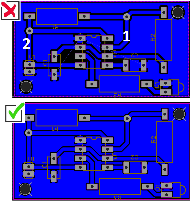
In the example at the top, area 2 is trapped along the left edge by the tracks that ring it. It never reaches area 1. Three ways out, in this order of preference: move a component to open a passage, redraw a track differently, or as a last resort reduce the clearance in the design rules. Never go below 0.5 mm, which is the limit of the cutter.
Tip
The ground plane is redone at every change. As soon as you move a component or a track, delete it and create it again. It is instantaneous, and a ground plane computed on the old routing no longer means anything.
19. Having the board checked by the software
Design → Check DRC. The DRC, for Design Rule Check, reads your board again and confronts it with the design rules set in section 11.
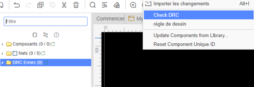
If it finds anything, the list appears on the left and each error is marked with a cross on the board. Click a row to be taken to the offending place.
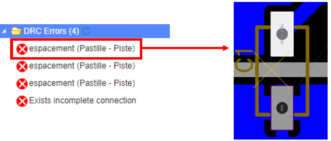
Two families come up all the time:
espacement (Pastille - Piste), that is pad to track clearance, means two coppers are too close to each other. Fix it by moving the track away, not by loosening the rule;Exists incomplete connectionmeans there is a ratsnest connection left that you have not drawn. It is often an isolated ground island, so read the previous section again.
Warning
The DRC only checks the drawing. It verifies distances and missing connections, nothing else. It will never tell you that your circuit is wrong, that you have swapped two pins or picked an absurd resistor. A DRC with zero errors means “this board can be manufactured”, never “this circuit works”.
Fix, redo the ground plane, run the DRC again. Repeat until zero.
20. The paper print, the last net before the copper
Before you start milling, there is one check left that costs no more than a sheet of paper: print the board at 1:1 scale and lay the real components on it. Better to lose an A4 sheet than a copper blank.
Fichiers → Exporter → PDF, that is File → Export → PDF.
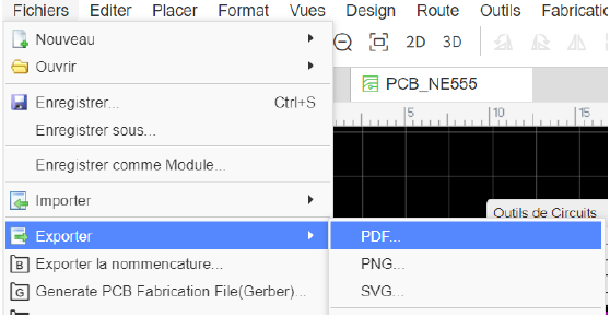
The export window asks which layers to output. What matters: Taille 1:1, the type Couche fusionnée, the colour Noir sur blanc, and the layers Côté Cuivre, BoardOutLine and Trous ticked. That is 1:1 size, merged layer, black on white, copper side, board outline and holes.
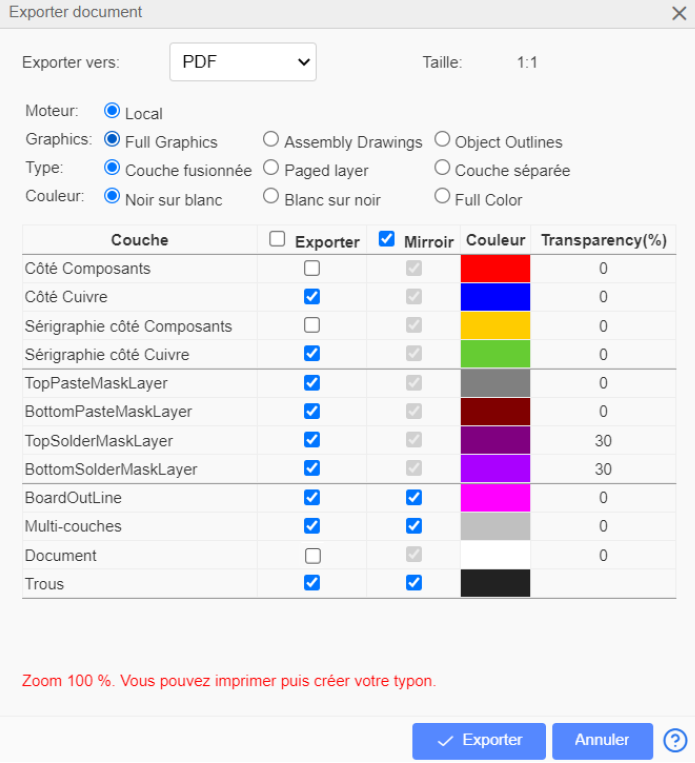
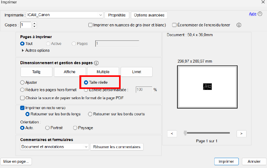
At the printing stage, one setting alone matters, and it is the one everybody gets wrong: tick Actual size, never Fit. A board printed “to fit” on the page proves absolutely nothing.
Then lay your components on the sheet, by transparency against a window or a lamp, and check that the leads fall into the holes. This is the footprint check of section 3, for real, and it is the last moment when a mistake is still free.
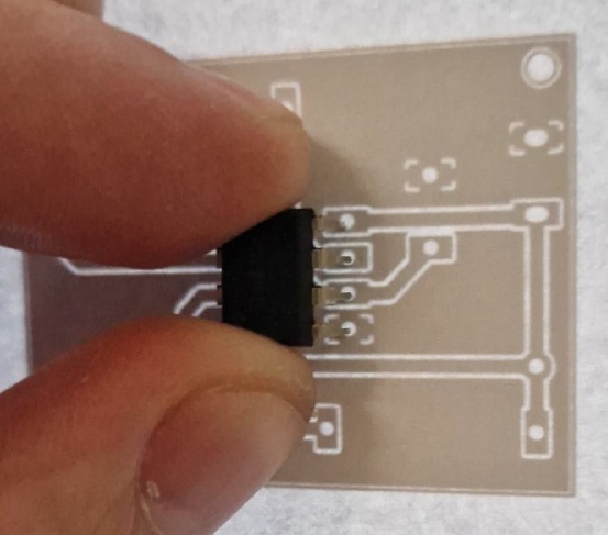
The component is at its real size, and so is the print. If the leads fall opposite, they will fall opposite on the copper. If they do not, you have just saved a blank.
21. Why you have been working mirrored from the start
One point that throws people, and that is better understood before soldering.
The copper is underneath the board, and the components sit on top. What you have been looking at on screen since the beginning of the session is therefore the copper face seen through the board, that is to say mirrored relative to the face where you will put the parts.
That is why the workshop flips the drawing before milling. Once the board comes out of the machine, it is the right way round for soldering. You have nothing to do about it, you just need to know, so as not to be surprised when your board looks “backwards”.
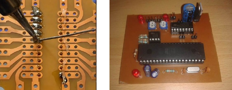
Soldering is therefore done on the copper side. And once the board is turned over, no track is visible any more. They are all underneath.
Sharing a project
Your board is finished. All that is left is to get it out of the software.
In offline mode, everything lives in a folder on your machine. Nothing is saved anywhere else, nothing is shared on its own. So the same gesture serves three purposes: handing in your work, passing it to a project partner, and backing it up before doing something silly.
Fichiers → Exporter → EasyEDA, which produces a .json file.
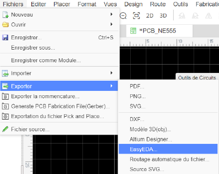
That .json is self-contained: it carries the symbols and the footprints of your components, including those that came from Contributions des utilisateurs. Whoever opens it therefore has nothing to download, even if they have never seen those parts.
Note
This is not a Gerber. The industry standard exchange format is the Gerber, and you will indeed find it in the same menu. But the school workshop works from the EasyEDA
.json, so that is the one we hand over. See the printed circuit board hub for the general vocabulary of manufacturing.
Attach your schematic to it, without which nobody can read back what the board is supposed to do.
Tip
Export before every big change. Offline mode has no history. If you break your board while trying to improve it, there is no button to go back once the software has been closed. A dated
.jsonin a corner of your disk is the only backup you have.
What comes next
You have taken a board from the first stroke of the schematic to the manufacturing file. What is left to do no longer happens in front of a screen. The blank comes out of the milling machine, you solder your components, you plug in the terminal. And the LED blinks, or it does not.
If it does not blink, the fault is almost never in the board. It is in a cold solder joint, an LED fitted the wrong way round, or a resistor value that was not the one you thought. The board itself has already been checked three times, at the DRC, at the paper print, and by the workshop.
See also
- Printed circuit board — the hub: vocabulary, general flow, and choosing a design tool
- KiCad — the other tool on the course, aimed at external manufacturing
- Reading a datasheet — to check the dimensions of a footprint
- Reading a schematic — reading and placement conventions
- Circuit simulation — trying a circuit out before routing it
- Soldering — what comes next, once the board is milled
Pitfalls
My board is milled, but I cannot solder one of the components
Check its footprint. It probably has no holes. You picked a surface mount part, and the workshop has no way of soldering it.
There is no clean recovery at this stage. Go back to the schematic, replace the part with a through-hole equivalent, with a
THorDIPfootprint and drilled pads in the preview. Then remake the board.It is the second most frequent source of error on this exercise, just after online mode. It takes two seconds to prevent when choosing the component, and costs a copper blank when forgotten.
A whole class is missing from the component search
You have gone back to connected mode without noticing. The software gives no warning. It lets you work, and the gap only shows up later, when you go looking for a component. The Contributions des utilisateurs class has vanished from the classes row.
Look at the title bar, at the top left. The words
Projects Offline modemust be there. If they are not, go back through Réglages → Desktop Edition Setting… → Run Mode Setting…, chooseProject Offline Mode,Apply, and restart the software.