Designing the electronics is the third step of building the embedded subsystem. Your board is chosen (step 2). What you now have to do is draw the circuit around it — connect the sensors and actuators chosen at step 2, match the logic levels, distribute the power, protect the inputs — then check it by calculation and simulation before you solder anything at all. The deliverable is an approved circuit schematic, ready to go to the printed circuit board.
The right mindset
There are two temptations: rushing towards the physical board (the printed circuit board) before the schematic is right, or copying a schematic from a tutorial without checking that it works with your board and your components. A schematic is not a drawing, it is a piece of reasoning: every connection on it is justified by a voltage, a current, a protection. You only freeze it once every interface has been checked, never before. A schematic error found after the board has been made (a burnt input, an undersized rail) is paid for in rebuilt boards. The same error found on paper is fixed in a minute.
Goal of this step
Produce an approved circuit schematic that:
- connects every sensor and actuator listed in the interface inventory (step 1 below) to the board you chose;
- guarantees logic level compatibility between the board and every peripheral;
- distributes power through properly sized rails, regulated and decoupled, with a ground that has been thought through;
- protects the sensitive inputs and the loads (diodes, pull resistors, current limits);
- has been checked by calculation or simulation wherever you were unsure;
- is frozen and ready to go to the printed circuit board.
Method
1. Inventory the interfaces
Before you draw a single wire, list exhaustively what your board has to connect. Two inputs come together here: the list of figures from scoping the embedded need (how many motors, sensors, contacts, what operator interface) and the pinout of the board chosen at step 2. For each connection, note the kind of signal (logic, analog, power), its voltage, its current and its frequency. The datasheet of each component gives you those figures. Schematic analysis gives you the symbols and conventions.
This inventory is your map of the interfaces: it says what to connect before saying how. Any connection left out here becomes a missing wire on the printed circuit board.
Example: 3-axis arm project
The arm uses three steppers driven by driver boards, three angle sensors, six limit switches and a serial console to the PC. The final operator link is over Wi-Fi: being wireless, it adds no interface to wire up. Inventory of the interfaces around the ESP32 (3.3 V logic):
Connection Kind Voltage Current / frequency 3 stepper drivers (STEP, DIR) logic (pulses) 3.3 V signal, ~20 kHz max 3 angle sensors analog 3.3 V 1 reading / 10 ms 6 limit switches logic (on/off state) dry contact event-driven Stepper coils (through the drivers) power 12 V ~1 A per phase PC console (debugging) serial 3.3 V 115 kbit/s Output: 5 families of connections, of which only one carries power (12 V) and only one needs matching (the limit switches). This inventory drives steps 2 to 4.
Deliverable 1/5 — Table of components to interface
- The interface inventory: for each connection, kind of signal, voltage, current, frequency
2. Match the logic levels
Every connection in the inventory joins two worlds that do not necessarily run at the same voltage. Your microcontroller usually works at 3.3 V. A sensor may output 5 V, a power stage lives at 12 V. For each connection, compare the voltage on the microcontroller side and on the peripheral side, then choose how to match them when they differ: a direct connection when the voltages agree, a voltage divider to bring an output down to an input, a level shifter for a bidirectional or fast connection, an optocoupler to isolate power from logic. Logic levels covers these arrangements and their limits.
Watch out
A 3.3 V input does not survive a 5 V signal. Putting a voltage higher than its own supply on a logic input makes its internal protection diodes conduct, then destroys the input stage. That destruction is often silent, the fault only showing up in use. Bring every incoming signal into your microcontroller’s range before it reaches the pin, never after.
Tip
You are allowed not to know, not allowed not to test. First time you meet a level shifter or an optocoupler? Build it on its own on a breadboard and check it with a meter before it goes on the schematic: it is the hardware equivalent of a unit test. And start from the datasheet: it almost always gives you the reference wiring arrangement (typical application), a safer starting point than a tutorial.
Example: 3-axis arm project
The five families of connections reviewed: only one needs matching, and power never touches the microcontroller.
Connection MCU side Peripheral side Matching STEP/DIR drivers 3.3 V GPIO outputs inputs that tolerate 3.3 V direct Angle sensors 0–3.3 V ADC inputs 0–3.3 V output direct Limit switches 3.3 V GPIO inputs contact to the pull voltage pull-up to 3.3 V PC console 3.3 V UART (TX/RX) USB-to-serial bridge on the dev board direct (built into the board) Stepper coils — (never connected to the MCU) 12 V handled by the driver Output: no incompatibility left, as long as the limit switches are pulled up to 3.3 V, and not to 5 V, a classic trap avoided by design.
Deliverable 2/5 — Table of logic levels
- The level matching table: for each connection, the voltage on both sides and the matching arrangement chosen
3. Distribute the power
Your components are connected and compatible. What is left is to power them. Design the power tree, from the source down to the components: a source (battery, mains adapter), one or more regulated rails (often 12 V for power, 5 V and 3.3 V for logic), the decoupling (capacitors as close as possible to each circuit, to absorb current surges), and a ground thought of as a network rather than as a wire. For each rail, work out a current budget: the sum of what the powered components draw, plus a margin. Designing a power supply covers regulation, sizing and battery life.
Watch out
Missing decoupling and a badly thought-out ground are the two most expensive power supply mistakes. Without a decoupling capacitor near a microcontroller, the current surges from switching pull its supply down and cause erratic resets, impossible to diagnose in the code. A ground shared between power (motors) and logic brings motor noise up into your analog readings: separate the two grounds and join them at a single point (star ground).
Example: 3-axis arm project
Power tree of the arm, starting from a 12 V source:
Rail Voltage Powers Current budget Power 12 V 3 stepper drivers (coils) ~3 A Logic 5 V (regulated down from 12 V) VIN input of the ESP32 board ~0.6 A Microcontroller 3.3 V (regulated down from 5 V, on the board) ESP32, angle sensors, limit switch pull-ups ~0.5 A (Wi-Fi peaks) Power and logic grounds separated, joined at one point near the source. 100 nF decoupling at every supply pin of the ESP32 and of the drivers.
Output: three rails, current budget worked out, regulators chosen (12→5 V external, 5→3.3 V on the board itself), star ground. This power arrangement folds into the main schematic.
Deliverable 3/5 — Power schematic (logic and power)
- The power schematic: source → rails tree, regulation, decoupling, ground, and the current budget for each rail
4. Protect and harden the wiring
A schematic that connects and powers everything correctly can still destroy its components at the first incident. Add the protections: a flyback diode on any inductive load you switch (relay, brushed DC motor) to absorb the spike at turn-off, usually built into stepper drivers but required for a coil you drive yourself; pull resistors (pull-up / pull-down) to set the level of floating inputs (a button, a limit switch); a current limit on outputs that drive LEDs or loads; input protection (series resistor and clamping) as soon as a wire leaves the board. These arrangements belong to schematic analysis and to logic levels.
Tip
Put your protections on the schematic, not as a patch on the finished board. Adding a flyback diode or a pull-up afterwards, on a board already laid out, means unreliable flying wires. Thinking the protections through on the schematic costs one symbol. Adding them later costs a board revision.
Example: 3-axis arm project
Protections chosen for the arm:
What is protected Risk Protection Stepper coils spike at turn-off built into the drivers (flyback) Limit switch inputs floating level, bounce 3.3 V pull-up + light RC filtering Sensor inputs (long wires) interference, spikes series resistor + capacitor 12 V supply reverse polarity series diode at the input Output: every input has a defined level at rest, every inductive load is protected, the supply is protected against reverse polarity. The schematic now stands up to the usual incidents.
Deliverable 4/5 — Circuit protections
- The protections built into the schematic: flyback on inductive loads, pull resistors on inputs, protection of exposed inputs and of the supply
5. Check, freeze, move to the PCB
Your schematic is complete. Before you freeze it, check the points you are unsure about. Not everything can be worked out in your head: a voltage divider under load, a regulator at its current limit, a power-up transient are all checked by simulation. Do not simulate everything, only what you are unsure of. Once every doubt is settled, freeze the schematic: that is the version that goes to layout, the routing of the tracks. The printed circuit board turns that frozen schematic into a manufacturable board. Any later change to the schematic forces you to redo the layout, which is exactly why you freeze only once you are sure.
Watch out
Laying out the board before the schematic is frozen loses you the layout. Every correction to the schematic after routing has started invalidates part of the layout. Freeze the schematic first, lay out second. And only simulate what you are unsure of: simulating an obvious arrangement wastes time, not simulating a doubtful one wastes a board.
Example: 3-axis arm project
Two uncertain points in the arm’s schematic, checked in simulation before freezing:
- The limit switch pull-ups: simulation of the arrangement (3.3 V pull-up + RC filtering) to check that the low level is clean and that the response time stays under 5 ms despite the filter. Result: low level at 0.1 V, response in 1.2 ms — within spec.
- The 5→3.3 V regulator under a Wi-Fi peak: simulation of the voltage drop during a 0.5 A demand. Result: an 80 mV dip, inside the ESP32’s tolerance.
Output: both doubts settled, the schematic is frozen and handed over to layout.
To pull it together, the arm’s reference schematic, annotated with the five layers of the method:
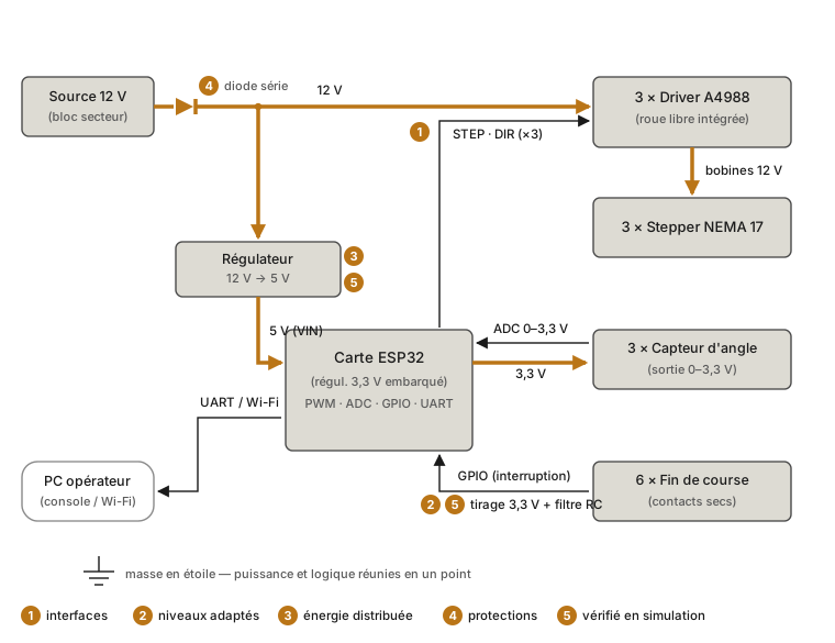
Deliverable 5/5 — Circuit schematic
- The approved circuit schematic: complete, checked in simulation on the uncertain points, frozen and ready for the board layout
Wrap-up
Your schematic is approved: interfaces inventoried, levels matched, power distributed, protections in place, uncertain points simulated. Next comes programming the firmware that will bring this hardware to life, and the physical build of the board (layout, manufacturing, soldering). Running this step — the schematic review, updating the parts list, the procurement schedule — is carried by the technical design file of the V-model.
Common pitfalls
Laying out the board before the schematic is frozen. Every correction to the schematic invalidates part of the routing already done. Freeze the schematic first, lay out second.
Copying a tutorial schematic without checking the voltages. An arrangement found online assumes its components and its board. Set every connection against the real voltages in your inventory before adopting it.
Forgetting the decoupling. Without a capacitor near the supply pins, switching pulls the voltage down and causes erratic resets, a fault you will hunt for in vain in the code.
Skipping the flyback diode on an inductive load. A coil switched off abruptly generates a spike that destroys the switching component. Any inductive load you drive directly needs its flyback.
Sharing one ground between power and logic. Motor noise then comes up into your analog readings. Separate the power and logic grounds, join them at a single point.
Simulating everything, or simulating nothing. Simulating an obvious arrangement wastes time. Not simulating a doubtful one wastes a board. Aim at what is uncertain, and only at that.
What belongs elsewhere
Running the step belongs to the V-model. The schematic review, its place in the parts list (BOM), the component ordering schedule belong to the technical design file. This page produces the artefact, the V-model puts it into the project.
The physical build of the board — etching or ordering the printed circuit board, drilling, soldering, inspection — is not covered here: it belongs to the electronics lab sessions and to our colleagues’ manufacturing course. This page stops at the frozen schematic and the logical layout.
The eco-design impact of the component choices (power draw, lifetime, repairability) and electrical safety (protection, low-voltage compliance) are arbitrated at project level: see eco-design and safety and quality.
See also
- Building the embedded subsystem
- Previous step: Choosing the hardware
- Next step: Programming
- Analysing a circuit schematic
- Logic levels
- Designing a power supply
- Circuit simulation
- Printed circuit board
- Technical design file (project management, V-model)
- Electronics manufacturing course (colleagues)