Going down to the register means driving the STM32 by writing straight into its hardware registers (GPIOA->ODR, RCC->AHB1ENR…), beneath the HAL and the LL. It is the lowest level reachable in C, the one the HAL hides: you gain in performance, determinism and understanding, you lose in comfort and portability. It is also the direct proving ground of bit manipulation: masks, shifts, |=, &= ~, ^= become concrete here. You go there out of need, not on principle.
What is it for?
The HAL is enough for most of a project. Four reasons justify going lower:
- Performance. Toggling a pin through the register takes a few cycles, where the HAL takes many more (checks, handle indirection). For a tight loop or a fast signal, the gap counts.
- Determinism. A register access has a known, stable duration, valuable for fine real-time work.
- Memory footprint. Without the HAL’s code, the binary is smaller, useful on chips with very little Flash.
- Understanding and unblocking. Reading what the HAL really does helps with debugging, and when a hardware setting is not exposed by the HAL, the register is the only way in.
The flip side: register code is specific to the chip (it does not carry over as it stands from an F4 to a G0) and less readable. It is a targeted tool, not a way of life.
Registers through CMSIS
You do not write memory addresses by hand. CMSIS (the standard ARM layer, shipped by ST) defines headers (stm32f4xx.h and the like) that describe every peripheral as a structure pointing at its registers. Writing GPIOA->ODR amounts to reaching the output register of port A, at the right address, without knowing it. These structures are declared volatile: the compiler must neither remove nor reorder those accesses (a register can change “on its own”, on the hardware side).
CMSIS also provides named bit macros — RCC_AHB1ENR_GPIOAEN, GPIO_MODER_MODE5_0, GPIO_BSRR_BS5… — which you use instead of magic numbers. This is exactly the discipline of bit manipulation: a named mask is worth more than an unreadable 0x00000400.
Info
The exact names of the macros depend on the family and the version of the CMSIS header (
GPIO_MODER_MODE5_0on recent versions, sometimesGPIO_MODER_MODER5_0on older ones). When in doubt, open the header of your chip (Ctrl+clickon the name in CubeIDE) to check the spelling and the field aimed at.
The canonical example — the bare-metal blink
Making LD2 (pin PA5) blink without the HAL, register by register, is the “Hello World” of low-level work. Three gestures:
/* USER CODE BEGIN 3 */
// 1. Power the clock of port A  (otherwise anything written into GPIOA is ignored!)
RCC->AHB1ENR |= RCC_AHB1ENR_GPIOAEN;

// 2. Set PA5 as an output: field MODE5 = 01
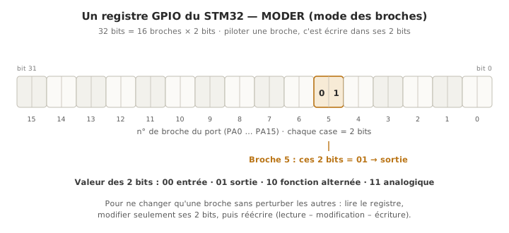
GPIOA->MODER &= ~GPIO_MODER_MODE5;     // clear the 2 bits of the field
GPIOA->MODER |=  GPIO_MODER_MODE5_0;   // set the low bit -> 01 = output

// 3. Blink through BSRR (atomic)
while (1) {
  GPIOA->BSRR = GPIO_BSRR_BS5;         // drive PA5 to 1
  for (volatile int i = 0; i < 800000; i++);   // rough delay
  GPIOA->BSRR = GPIO_BSRR_BR5;         // drive PA5 back to 0
  for (volatile int i = 0; i < 800000; i++);
}
/* USER CODE END 3 */
You recognise the grammar of bit manipulation: |= to set a bit, &= ~ to clear one, named masks everywhere. Compared with the HAL’s single HAL_GPIO_TogglePin(LD2_GPIO_Port, LD2_Pin), it is longer, but you see exactly what the hardware does. The for loop on a volatile counter is a crude delay (to be banned in real code, where you use a timer). Here it is only there to make the blinking visible.
Take a screenshot of the Debug perspective of CubeIDE, with the Registers view open on GPIOA, where bit 5 of the ODR register toggles at every execution step, as a GIF, the movement being the message.
BSRR versus ODR — atomicity
Two ways of changing the state of a pin, and they are not equivalent:
- Through
ODR:GPIOA->ODR |= GPIO_ODR_OD5;. This is a read-modify-write (the|=reads the register, changes one bit, writes the whole thing back). If an interrupt changes another pin of the same port between the read and the write, its change is lost. Not atomic. - Through
BSRR:GPIOA->BSRR = GPIO_BSRR_BS5;, a single write, atomic. The low 16 bits set to 1, the high 16 bits reset to 0. Bits that are not aimed at are left untouched. No race is possible.
The rule: prefer BSRR to set or clear a pin, especially if interrupts touch the same port. It is a textbook case of atomicity, extending bit manipulation directly.
The Reference Manual, not the datasheet
The source of truth for low-level work is the Reference Manual (ST’s RM0xxx document): it describes every register, every bit field, their address and their effect. Not to be confused with the chip’s datasheet, which gives the pinout, the electrical characteristics and the limits (see reading a datasheet). To write a register, it is the Reference Manual that you open, often alongside the CMSIS header, which is its translation into macros.
Pitfalls
Forgetting to power the peripheral’s clock. The number one trap of low-level work: writing into GPIOA (or any other peripheral) without having enabled its clock in RCC beforehand. The writes are silently ignored, without any error. Always start with the RCC->...ENR |= ..._EN.
Non-atomic read-modify-write. Using ODR |= / ^= where an interrupt touches the same port: the change is lost. Prefer BSRR.
Magic numbers instead of macros. Writing 0x400 rather than GPIO_MODER_MODE5_0: unreadable, brittle, wrong as soon as you change pin. Use the CMSIS macros: that is the lesson of bit manipulation.
Forgetting volatile. If you build your own register pointer (instead of going through CMSIS), not declaring it volatile lets the compiler optimise the accesses away, and the code “works in debug, not in release”. The CMSIS definitions are already volatile.
Believing the code is portable. A register blink written for an F4 does not build as it stands on a G0: the bus names (AHB1ENR vs IOPENR), and sometimes the fields, differ. That is the assumed cost of leaving the HAL.
Exercises
Exercise 1 — The silent blink
A student copies steps 2 and 3 of the bare-metal blink (MODER then BSRR) but leaves out step 1. The code builds, flashes, but the LED never lights. Why, and what should be checked first?
Solution
Without
RCC->AHB1ENR |= RCC_AHB1ENR_GPIOAEN, port A is not powered: every write intoGPIOA->MODERandGPIOA->BSRRfalls into the void, with no effect and no error. That is the reflex to have in front of a low-level peripheral that “does not answer”: check first that its clock is enabled in RCC. The HAL does it automatically (insideMX_GPIO_Init), which hides this trap, hence its painful discovery when moving to the register.
Exercise 2 — Why BSRR?
An LED is on
PA5, and a fast interrupt togglesPA6of the same port throughGPIOA->ODR ^= GPIO_ODR_OD6. In the main loop, you writeGPIOA->ODR |= GPIO_ODR_OD5to light the LED. Which bug can occur, and how do you avoid it?
Solution
The
|=of the main loop makes it readODR, set bit 5, write back. If the interrupt onPA6happens between the read and the write-back, its toggling ofPA6is overwritten by the write-back of the old value: the state ofPA6is corrupted intermittently (a bug that is very hard to reproduce). The solution: useBSRRon both sides:GPIOA->BSRR = GPIO_BSRR_BS5in the loop, andBSRRin the interrupt too. Every BSRR write is atomic and touches only its own pin, removing the race. It is the concrete illustration of the atomicity seen in bit manipulation.
Where it fits in the project
- Step 4 of the proof-of-concept phase. Going down to the register is a targeted optimisation, not the starting point: you prototype with the HAL, and you only “register” the critical path you have identified (a signal that is too slow, a footprint that is too large). A PoC that starts straight at low level loses time without any gain.
- A deliberate mix. Common practice is to configure with CubeMX and the HAL, then to replace with register accesses only the few lines where performance demands it. The rest stays readable and portable.
Understanding registers, even without using them day to day, demystifies the HAL: you now know what it does “underneath”, and you choose knowingly which level to write each part of the firmware at.
Going further
- Bit manipulation — the cross-cutting notion this page puts to work: masks, shifts, atomicity.
- Programming with the HAL · Configuring with CubeMX — the layers above, and where the clock init comes from.
- Reference Manual of your chip (
RM0xxx, onst.com) — the exhaustive description of the registers.
See also
- STM32 — hub of the STM32 tutorials
- Programming with the HAL — the layer above, the usual starting point
- Bit manipulation — masks and bits, the cross-cutting base of this page
- Reading a datasheet — and how it differs from the Reference Manual
- Timers — the right way to wait, rather than a
forloop (cross-cutting)